Application EP3364729 relates to the improvement of heat dissipation on a printed circuit board (PCB).
Brief outline of the case
The application was refused for lack of IS and lack of clarity.
The applicant appealed.
In appeal, the MR was not allowable under Art 123(2) and AR 1 and 2 not admitted under Art 13(2) and 13(1) RPBA. The application was thus refused for good.
The case is interesting in view of the objections under Art 123(2). They relate to the relative size of the pad (16) and the HDSMC (15) mounted thereon.
The applicant’s point of view
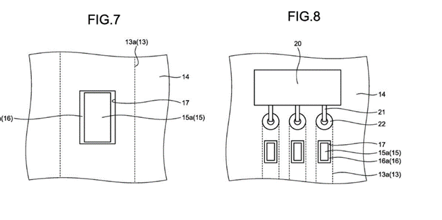
The applicant argued that the skilled person would directly and unambiguously derive features (M) and (N) in their broad meaning from Figures 7 and 8 if they knew features (M) and (N) from the description of Figures 2 to 6.
Feature (M) defines that the pad portion is larger than the bottom surface of the HDSMC.
Feature (N) defines the necessary and sufficient condition that a part of the pad portion does not have an HDSMC mounted thereon.
Claim 1 is based on the description of Figures 7 and 8, which was very broad and thus included every shape, size and arrangement of the pads or HDSMCs.
Based on this broad description, the skilled person would therefore deduce that, despite the representation of precise shapes, sizes and arrangements of the pads/HDSMCs, every shape, size and arrangement of the pads/HDSMCs was included by the inventive concept.
The description was suitable for extracting individual features from the embodiments and including them in the independent claim. The skilled person knew that features (M) and (N) were independent of the other features, which were not essential for the invention, and that they were also not functionally related to these other features. Therefore, feature (M)/(N) could be isolated from the detailed embodiments of Figures 2 to 6 and derived directly and unambiguously in their broad terms from the disclosure of the drawings. The skilled person would infer the general meaning of features (M) and (N) in view of the schematic drawings of Figures 7 and 8.
The effect of the difference in size between the bottom surface of the HDSMC to be soldered and the pad portion was both a better heat dissipation through the exposed part of the pad portion and better fitting of the HDSMC by providing a clearance for fitting the HDSMC, i.e. by minimising the risk that the HDSMC was partially mounted on solder resist. The skilled person knew how to design the pads such that these effects were achieved.
The board’s decision
Certain features (H), (L), (M) and (N) of the originally filed independent claim have been amended. During the OP before the board mainly the basis for features (M) and (N) in the application as filed were discussed.
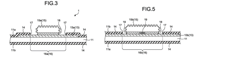
Feature (N) allegedly has a basis in the respective last sentence of paragraphs [0035] and [0036] of the application as filed. Both sentences have very similar content and refer to HDSMCs 15a and 15b.
The embodiments of Figures 2 to 6 contain many details about the PCB and its manufacture.
The feature (M)/(N) is mentioned in the context of the mode of action of the structure of the very special arrangement of Figures 2 to 5. This effect and function, namely the partial dissipation of heat by the pads 16, is only achieved for the special relative dimensions of pads 16 and HDSMCs 15 shown in Figures 2 to 5 and not for any arbitrary structure, e.g. if the pads are only infinitesimally larger than the bottom surface of the HDSMCs.
For the board, the feature (M)/(N) is very strongly embedded in the specific embodiments of Figures 2 to 6 and cannot be transferred in its general and broad meaning to the schematic and generalised representation of Figures 7 and 8 without resulting in a generalisation, which is not disclosed in the application as filed.
Despite the more generalised and simplified representation, the schematic drawings of Figures 7 and 8 still contain certain specific features, such as the shape and relative sizes of the pad portions 16 and HDSMCs 15 and also of the wiring 13 forming the pad portions 16, which in turn depend on the type and size of the large-current electric component 20.
Feature (M)/(N) is very broad in that it leaves completely open the shapes of the pad portion, the HDSMC and the non-covered part of the pad portion as well as the difference in size between the bottom surface of the HDSMC to be soldered and the pad portion (between infinitesimally small and very large as no relative relationship or e.g. order(s) of magnitude are given).
Moreover, improved heat dissipation through the exposed part of the pad portion and improved fitting of the HDSMC can only be achieved for a certain minimum amount of clearance, as shown schematically in Figures 7 and 8. Figures 7 and 8 also show both a certain (rectangular) shape of the pad portion 16 and that a distance to the solder resist 14 is maintained on all sides of the HDSMC.
These drawings also show that an arbitrarily large spacing is not possible, due to the limited space provided by the wiring 13, the dimensions and shape of which are determined by the size and spacing of the electrodes 21 of large-current electronic component 20. However, this spacing range or any detail in this respect is not reflected in features (M) and (N), and is not disclosed in the description of the application as filed, either.
In features (M) and (N), however, any shape and size of both the pad portion and the bottom surface of the HDSMC is possible as long as the former is larger than the latter. Furthermore, feature (M) also leaves it completely open whether the specified condition (“larger”) applies to only one, several or all sides of the pad portion 16 and similarly for feature (N).
The board was of the opinion that in order to avoid an extension of subject-matter beyond the content of the application as filed, at least these additional features of Figures 7 and 8 would have to be included in the claim wording.
For the board, the description of a drawing may thus be inextricably linked to the specific disclosure of this drawing. If a feature in the description of the drawing is extracted from the very specific context of the drawing in order to be included in a claim, the specific disclosure of the drawing must be taken into account.
If there is no literal support for this specific disclosure in the application as filed which could be used for supplementing the feature used for amending the claim, it may not be possible to avoid an unallowable intermediate generalisation. This may in particular occur if a feature from a specific and detailed embodiment is placed in the context of a schematic drawing.
The board further noted that the only option to arrive at a claim which does not extend beyond the application as filed would be to delete both features (M) and (N). However, this may well lead to an objection of lack of IS over document D2.
Therefore, a trap-like situation occurs because the features may not be removed from the claim as it would lead to lack of IS, while they may not be left in the claim due to added subject-matter because of an unallowable intermediate generalisation, and apparently cannot be supplemented with features that would avoid an unallowable intermediate generalisation, due to lack of explicit disclosure.
Comments
The decision is interesting in that it shows that in order to avoid objections of IS certain features of the drawings might have to be included in the claim. If those features are inextricably linked with other ones, there might be a trap-like situation.
On the other hand, extracting specific features from a drawing, without adequate support in the original disclosure, regularly endsup in an intermediate generalisation.
When the applicant uses the terminology “included by the inventive concept” he manifestly relies on the US way of allowing generalisations once the inventor “possesses the invention”. It might be obvious, but not directly and unambiguously derivable from the original disclosure…..
https://www.epo.org/en/boards-of-appeal/decisions/t210324eu1
Comments
2 replies on “T 324/21 – Trap-like situation between lack of IS and intermediate generalisation ”
Thank you, Daniel, for those comments and reference to “possessing” the invention. US law requires there to be a “written description” (WD) of the claimed subject matter in the application as filed. Many American patent attorneys do not understand our “added matter” issue but do understand the need for WD.
Interesting is that in reponse to an objection of lack of WD, Applicant’s burden to demonstrate adequate WD is not an obviosness test but, rather, a disclosure test. So a “lack of WD” objection is comparable with our Art 123(2) objections. In theory, that is. The practice is a bit different.
Dear Max Drei,
Thanks for your comment.
I got the notion of “possessing” the invention from listening to US patent attorneys about the different approach between the US and the EPO when it comes to added matter. The problem seems to me that a lot can be interpreted in a WD in the US, but not at the EPO. This explains to a large part of the difficulties experienced by US applicants when they come to the EPO. “Directly and unambiguously disclosed” is miles away from interpreting a WD.
The whole drafting and claim construction philosophy is so different in the US and in Europe. I therefore doubt that a common understanding on WD and added matter under Art 123(22) will ever be obtained. .